5-stage Pipeline RISC-V CPU
A SystemVerilog implementation of a pipelined RISC-V CPU.

View the GitHub repository here: RISV-V-RV64I
Preface
Done in collaboration with Mazda Farrahi and Faaiq Majeed. This showcases only a portion of a larger project, one that fully emulates the CPU using a synthesizable container module that utilizes HPS to FPGA communication for interfacing view it here. This project is still ongoing, however, this document will go over the significant amount of work already completed.
Summary
This is a SystemVerilog implementation of a RISC-V 64I (64-bit Integer) CPU that currently features a 5-stage pipeline. Future updates will include caching, and hardware support for MUL and DIV instructions.
The post outlines the CPU and its related modules, along with SystemVerilog testbenches that has validated each module throughout the design.
Contents
- Introduction
- Architecture
- Overall Structure
- Pipelined Datapath
- SystemVerilog Modules
- Data Storage
- ALU
- Control Module
- Hazard Detection Unit
- Forwarding Unit
- Testbenching
- Testing Approach
- Progress and Results
- Future Updates
- Conclusions
- References
- Bibliography
- Acknowledgements
1. Introduction
The objective of this project is to implement the RISC-V RV64-I (64-bit integer subset) ISA using SystemVerilog and to testbench all modules thoroughly. Specific design goals includes:
- Designing a synthesizable CPU that supports the base arithmetic operations along with store, load, and branching operations.
- Further extending the instruction set to include the full RISC-V RV64-I instruction set.
- To incorporate a 5-stage pipeline in the architecture.
- To incorporate caching in the architecture.
- Extensively validate each SystemVerilog modules to approach near 100% coverage in RTL simulation and synthesis simulation. As of the writing of this blog, our CPU currently supports the base arithmetic operations including store, load, and branching operations along with a 5-stage pipeline. We have also performed rudimentary tests. As this project is still in progress, other design goals will be fulfilled in upcoming updates.
2. Architecture
2.1 Overall Structure
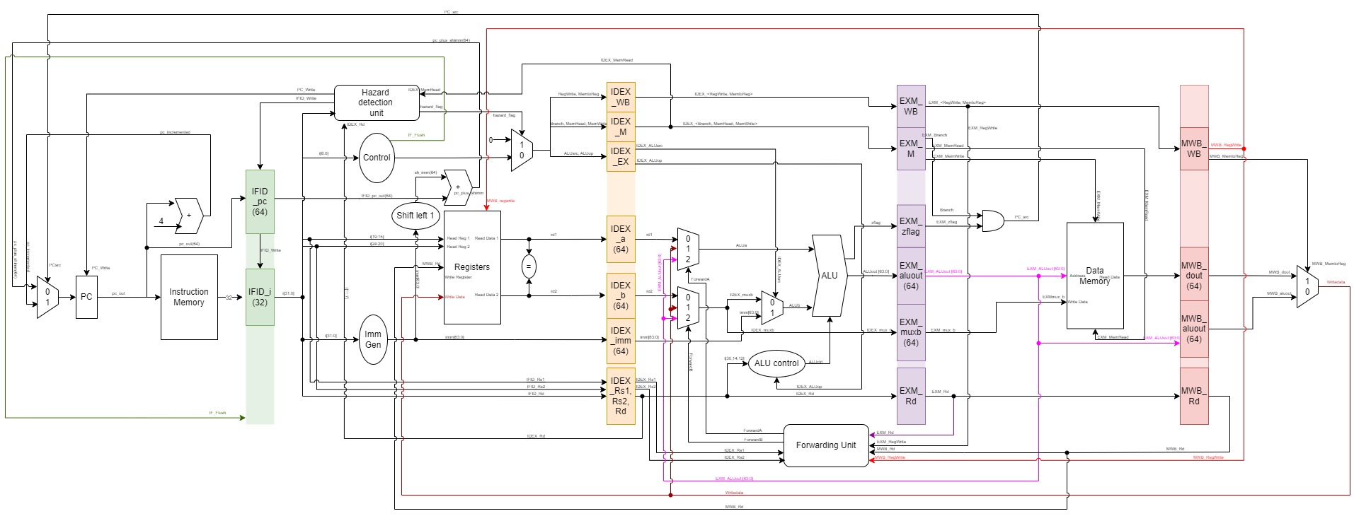
The Datapath can be found in cpu.sv in the GitHub repository. It is designed around the classic 5-stage pipeline model, consisting of the following stages:
- Instruction Fetch (IF)
- Instruction Decode (ID)
- Execute (EX)
- Memory Access (MEM)
- Write-Back (WB)
We ran rudimentary tests (testbench found under
\tests\pipeline_tb.sv) to ensure expected performance of this portion.
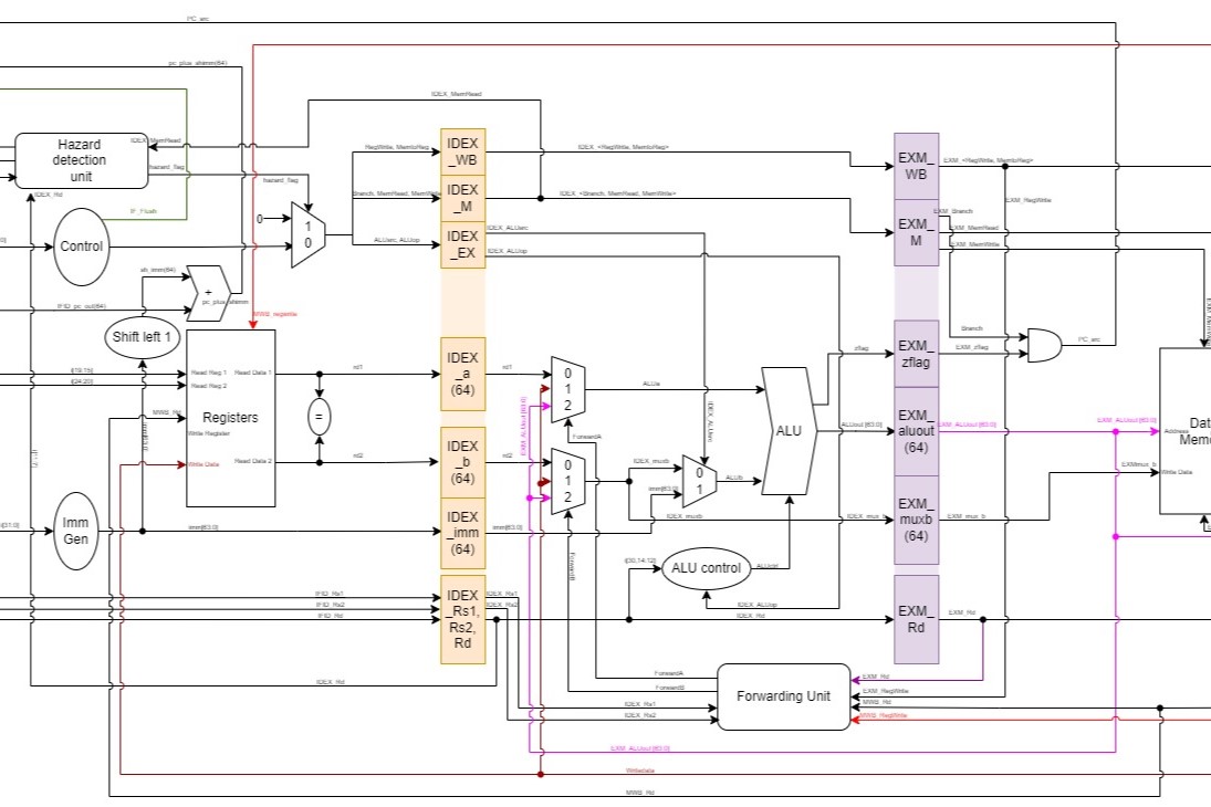
The following figure (Figure 1) shows the block-diagram of the architecture:
 ***Figure 1**: Block Diagram of the overall Datapath architecture.*
2.2 Pipelined Datapath
The SystemVerilog implementation of the pipeline is also illustrated in Figure 1. Each piece of data would have it's own D-Flip-Flop registers at the boundary of each stage. On the positive edge of clock, each piece of data would then propagate to it's corresponding register one pipeline stage away. An analogy one can try is by pretending pipeline registers to be water buckets, and the combinational logic between the registers to be paths and pipes that redirect/manipulate the water as it flows through. If the IF/ID buckets pours out it's water (on the clock signal's positive edge), the water would be get 'modified' before being collected in the ID/EX buckets.
Here's a snippet of the actual SystemVerilog:
/* Combinational logic above ^^^ that would have the processed data ready to be fed into the IDEX registers on posedge clk */

always @(posedge clk) begin    // ID ---> EX
    IDEX_Rs1 <= IFID_i[19:15]; // Rs1
    IDEX_Rs2 <= IFID_i[24:20]; // Rs2
    IDEX_Rd  <= IFID_i[11:7];  // Rd
    IDEX_a <= Regout1;
    IDEX_b <= Regout2;
    IDEX_ALUcontrol <= {IFID_i[30], IFID_i[14:12]}; // This is the input for the ALU Control module
    IDEX_imm <= imm;
    if(~hazard_flag)begin
        {IDEX_RegWrite, IDEX_MemtoReg, IDEX_Branch, IDEX_MemRead,
        IDEX_MemWrite, IDEX_ALUsrc, IDEX_ALUop} <= {RegWrite, MemtoReg, Branch, MemRead, MemWrite, ALUsrc, ALUop}; // Control Signals
    end else begin
         {IDEX_RegWrite, IDEX_MemtoReg, IDEX_Branch, IDEX_MemRead,
        IDEX_MemWrite, IDEX_ALUsrc, IDEX_ALUop} <= 8'b0; // Overrides Control Output to 0s when Hazard occurs.
    end
end
The non-blocking assignment <= is used to ensure that the signals propagate from stage to stage in parallel as soon as clock strikes a positive edge.
3. SystemVerilog Modules
3.1 Data Storage
The modules responsible for storing data are regfile, iMem (short for instruction memory), and dataMem (as in data memory).
They follow a conventional write enable protected, async read format. See the GitHub repository for the source code.
3.2 ALU
The Arithmetic Logic Unit (ALU) is fully combinational, and provides an additional zero flag as an output. Future updates will grant this module a negative and overflow flag.
3.3 ALUcontrol
Found in cpu.sv, this module is a intermediary module that sits between the ALU and Control module. In this implementation, ALU operations are first decoded by the Control Module and then fed into the ALUcontrol module. The purpose of this module is to be able to 'infer' the correct ALU operation based on the 32-bit instruction which has overlaps in regions, this module is able to ignore irrelevant bits and ensure the correct ALU operation.
3.3 Control Module
Found in cpu.sv, this module takes in the opcode from the 32-bit instruction and sends the appropriate control signals to toggle other modules, including ALUcontrol.
3.4 Hazard Detection Unit
Found in cpu.sv, this combinational module checks for pipeline hazards and conditionally stalls the pipeline by checking if the read register request from ID/EX stage matches the destination registers in the IF/ID stage. This way, read requests coming from further down in the pipeline would get the correct source register value from the current position in the pipeline.
3.5 Forwarding Unit
Found in cpu.sv, this combinational module checks for read requests from the EX/M stage and forwards any freshly computed values from the ID/EX stage. This way, the EX/M stage doesn't have to wait until this needed computed result to first be stored in the registers before being delivered. See the GitHub repository for the SystemVerilog source code.
4. Testbenching
4.1 Testing Approach
We hope to utilize UVM to test our modules. This is currently underway on certain modules, and will be presented in coming updates.
4.2 Progress and Results
Currently, only basic RTL tests were performed. More extensive testing are to come in future updates!
5. Future Updates
Planned updates include:
- Caching Mechanism
- Hardware support for
MULandDIVinstructions. - Dynamic Branch Prediction
6. Conclusions
The implementation of a 5-stage pipelined RISC-V 64I CPU in SystemVerilog demonstrates the feasibility of building a functional CPU core using modern hardware description languages. The modular design makes testing and future enhancements easier. The use of synthesizable testbenches ensures that the design is also viable for hardware deployment.
7. References
The RISC-V Instruction Set Manual SystemVerilog References by ChipVerify
8. Bibliography
Intel Quartus Prime Documentation
9. Acknowledgements
The two other project members involved are Mazda Farrahi and Faaiq Majeed (view Faaiq's GitHub repository of the assembler here: RISC-V Assembler). Both have contributed a significant amount of progress that made this project possible. Mazda and I specialized in implementing the hardware design while Faaiq programmed an assembler for this instruction set using C.